- Home
- Products

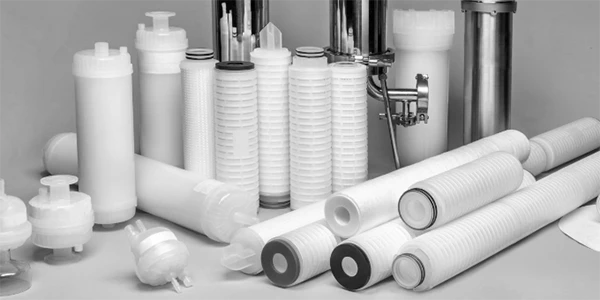
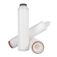
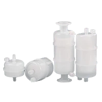
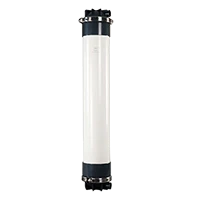
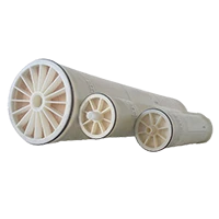
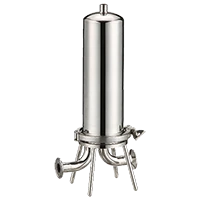
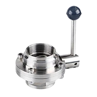
We provide a one-stop procurement service for sanitary grade filter materials and accessories, reducing your procurement costs.
Read More - Industries
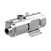
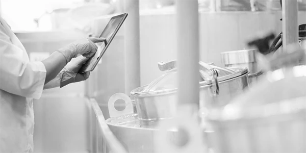
We specialize in providing filtration products and services for the microelectronics, biopharmaceuticals, and food and beverage industries with high hygiene needs.
Read More - Quality Assurance
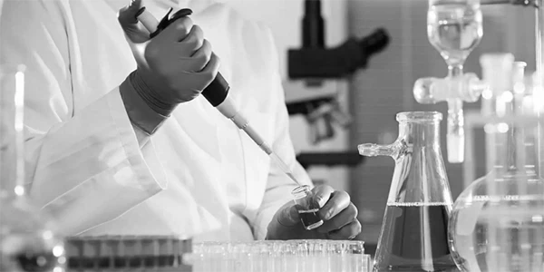
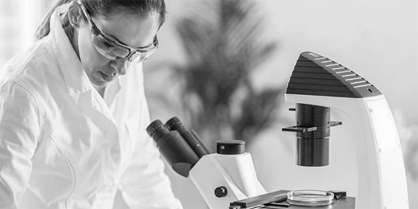
Quality is our mission, and it is our duty to ensure that our products meet industry demands.
Read More - Knowledge
Provide product selection guidelines and technical knowledge services to reduce your selection costs.
Read More - About
Welcome, we are a global supplier of sanitary filtration media and accessories, specializing in providing sanitary filtration solutions.
Read More - Contact